Common Challenges in Printed Circuit Board Assembly and How to Overcome Them
There are several common challenges that impact all PCB assembly. Some challenges are merely annoyances, while others can significantly impact performance. To overcome or avoid these challenges, partner with a quality ECM who can assist with the design process and address potential issues before they become problems.
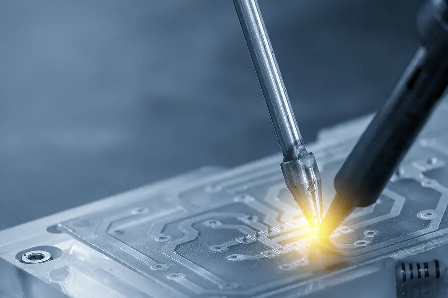
Defects in Soldering
PCB soldering defects are a common issue in PCB assembly. This can include gaps in the solder joints, cold solder joints, solder balling, solder bridging, a component shift, lifted pads, webbing and splashing, sunken joints, tombstoning, and shadowing. These defects can generate a range of problems, some are simple cosmetic defects, while others can cause functional failure. If the defect is severe, the board will need to be scrapped entirely, which can cause significant delays. Whenever a defect in soldering is detected, the process will need to be stopped and fixed, which can increase the cost of the assembly and the timeline to delivery. To avoid defects in soldering, a review of the design can take place before assembly to look for any potential problem areas that can cause a soldering defect. Prevention is the best cure for soldering defects. An ECM who takes a proactive approach to PCB design and has a rigorous testing program in place can help you overcome this challenge.
Incomplete or Improper Component Placement
Placing components too close to one another, oriented incorrectly, or in the wrong location on the board will cause issues during the manufacturing process. Component placement determines how a PCB is manufactured, and improper placement can dramatically increase the cost of the board. To avoid this issue, the board should go through a DFM (Design for Manufacturing) analysis prior to assembly. With this analysis, the right components can be selected and component placement can be optimized.
Board Warping
Board warping is the alteration of the PCB shape. This change in the PCB shape was not planned for, and therefore will cause assembly issues. With warping, the PCB will not remain flat, making it an inconsistent height, causing construction issues as the rest of the device comes together. Poor solder linking and damage to the components are both possible during assembly, and even if assembly is possible, the project can fail with a warped PCB. Board warping needs to be addressed early in the process. To avoid board warping, there needs to be balance in the board, which will be determined during the design phase. During construction, technicians should be careful not to apply too much heat or force, especially in thin areas. Having an experienced manufacturing team who knows how to avoid board warping can eliminate this issue.
Electrical Noise
Electrical noise is often produced by a bad board. In general, some noise is not a problem as long as it doesn’t interfere with system performance, but if it is not appropriately handled, it can have an impact on the operation of the board. Interferences from PCB noise can lead to issues in performance, particularly if the noises are high-frequency. Sometimes this noise is produced by spikes in electrical signals, which can be caused by incorrect ground connections. To remedy this issue, layout is crucial. The design of the PCB can make a big difference in the amount of electrical noise. The arrangement of the layers will determine the digital noise, and, if possible, ground planes should be included in the PCB layout to cover the board area. A strong design team of engineers can work during the design phase to ensure that noise is kept to a minimum.
Avoid These Challenges by Being Proactive
With a quality ECM who encourages a DFM analysis before PCB assembly, many of these common challenges can be avoided. A DFM analysis will look for potential issues before assembly begins and structure the component in a way that is optimal for manufacturing. Although this is an additional step in the process, it will save both time and money in the long run. A scrapped board or a redesign is often much more expensive and can cause significant delays. An experienced ECM will know where to look in the design and anticipate challenges before they become expensive problems.
Get Started NowPartnering with a turnkey electronic contract manufacturer offers multiple advantages. Specialized expertise ensures top-notch quality and efficiency, while cost savings result from their bulk material procurement and process optimization. ECMs expedite time-to-market by swiftly initiating production, freeing your focus for core competencies and innovation. They mitigate risks through ingenuity and stringent quality control. Scalability is simplified, eliminating heavy investments, and established ECMs guarantee reliable adherence to industry standards. Access to cutting-edge technology is an added perk, and customization capabilities can suit your unique product’s specific needs. As an industry leader, Levison Enterprises is a trusted partner for your next PCB project. Contact us for a quote today.