5 Historical Events That Shaped PCBs For Electronic Manufacturers
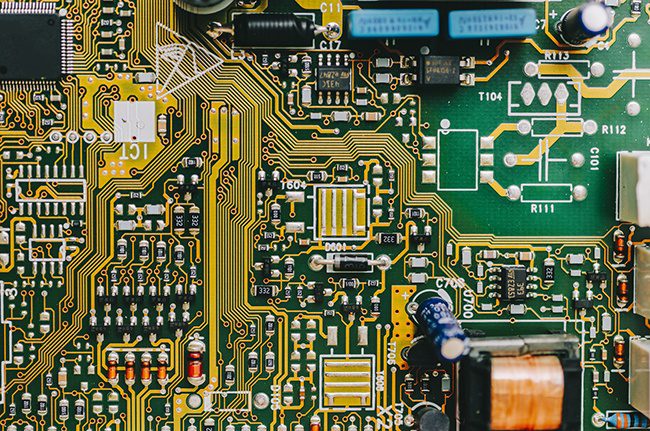
The printed circuit boards (PCBs) electronic manufacturers use today have evolved over the last 100 years and beyond. PCBs have an exciting history, borne first from the earliest ventures into electronics and later reimagined by a desire to revolutionize point-to-point wiring boards. Learning about the important events that molded the modern PCB can lend a better appreciation for this technology and an idea of what’s to come for the future of PCB assembly.
1. The First Long-Distance Radio Telegraph System
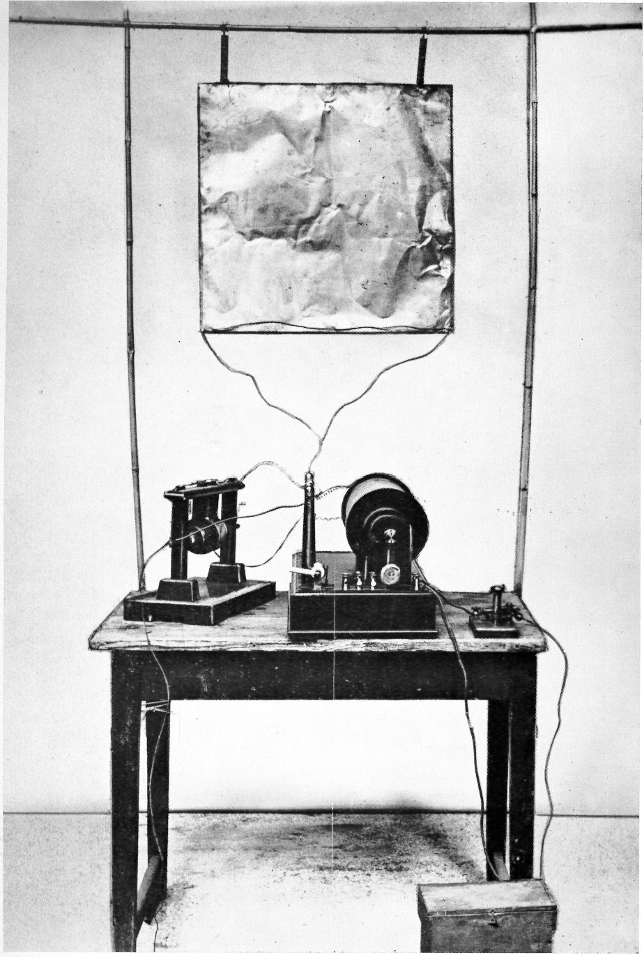
In 1895, an Italian physicist named Guglielmo Marconi made history by inventing the first successful long-distance wireless telegraph system. The creation of the long-distance radio telegraph presented a new system of communication – one that ended many perils of sea travel and saved hundreds of lives. For example, all the survivors of the sinking of the Titanic owe Marconi their lives, as it was his invention that enabled them to call for help.
Marconi created the invention after experimenting with a crude induction coil (to increase voltages), a spark discharger, and a simple coherer device or detector to pick up radio waves. He successfully transmitted messages using Morse code over short distances and eventually increased the range of signaling by testing with a vertical antenna. Marconi’s radio worked using a traditional point-to-point wiring system.
The point-to-point system used a design in which individual wires connected each component. The result was a large, bulky, unreliable device that often had poor connections. Marconi’s radio led to the creation of the first PCBs in the early 1900s, through the need to improve the complex point-to-point wiring system.
2. The Invention of the Printed Circuit Board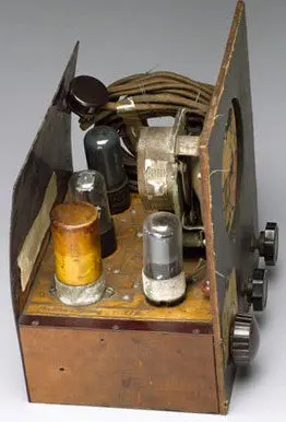
Paul Eisler, Viennese engineer and inventor, developed the first PCB in 1936. In the 1930s, printing was a successful and robust technology. Eisler imagined an electronic circuit created through the printing process – one that would eliminate the labor-intensive requirements of hand-soldering wires. His invention would bypass issues with point-to-point wiring by printing the wires onto an insulating base and then mounting the elements on top.
Eisler had a difficult life, leaving Austria and moving to England to escape Nazi persecution in 1936. Britain identified him as an enemy alien after WWII began, and he was behind bars until his release in 1941. After this, he found it difficult to secure a job in England and could not sell his printed circuit board idea to major communications companies.
Eisler continued to try to sell his inventions and managed to engage a lithography company in England called Henderson and Spalding. The company invested in the print circuit idea through a subsidiary called Technograph.
Unfortunately for Eisler, the contract he signed forfeited his rights to the invention. He received 16.5% ownership of the Technograph but agreed to submit any patent rights during his employment.
In 1843, Eisler patented the use of printed circuits (through Technograph) in many products, including motors, transformers, cables, aerials, and heated wallpaper. Still, there was no demand for printed circuits until Americans needed a way to improve a device called a proximity fuse, to bring down V1 rockets during the war.
3. Weapon Developments During World War II
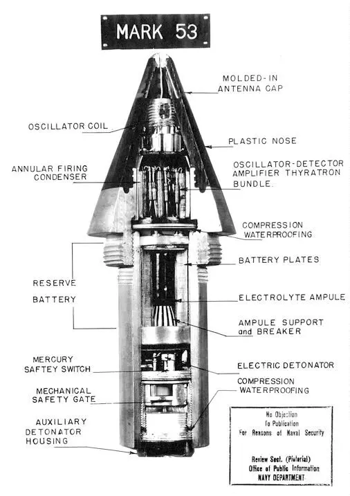
British military researchers invented the proximity fuse early in WWII. A proximity fuse detonates explosive devices automatically within a certain distance to the target. The British shared their initial designs with the United States, who helped design and manufacture the fuse.
Despite his previous failed negotiations, Eisler had obtained patents for other printed circuit boards applications including a radio design that featured his printed circuit board.
PCBs improved the design of proxy fuses by giving them the power of radio systems to track the path of the projectile and to emit radio waves that interacted with the target. The sophisticated trigger mechanism of the proxy fuse using PCB technology was incredibly important in WWII, and it later led to the U.S. mandating the use of PCBs in all airborne instruments in 1948.
4. The Invention of the PCB Auto-Assembly Process
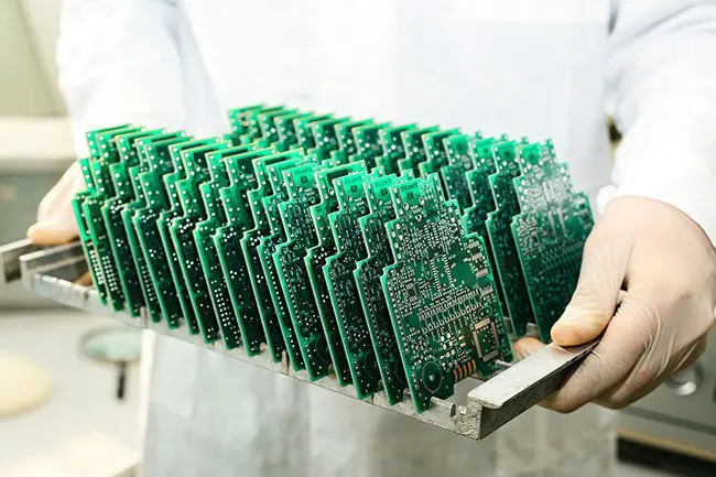
The first PCBs used “through-hole construction.” They used wire leads, with holes drilled into the board for the wire of each component. Early PCB materials (in the 1920s) were composed of anything from pieces of wood to Bakelite or Masonite – anything one could drill holes into and could rivet flat brass wires into. In 1947, the first double-sided PCBs with plated through-holes were made.
In 1949, two members of the U.S. Army Signal Corps (Moe Abramson and Stanislaus F. Danko) came up with the first PCB auto-assembly process, which used a copper foil interconnection pattern and dip soldering techniques to insert component leads onto the board. The process drew the wiring pattern and photographed it onto a plate made of zinc.
Then, developers used this plate to create a printing plate, which helped develop an easy offset printing process. It was officially patented in 1956 and would evolve into the PCB fabrication process we use today.
5. Improvements in PCB Design and Manufacture
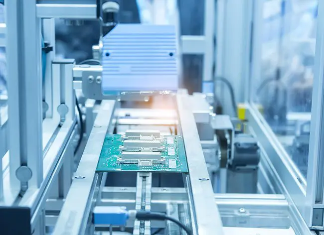
In the 1950s and 1960s, engineers continued to develop printed circuit boards using new materials and resins to print circuits more quickly, efficiently, and at higher volume. For the most part, PCBs during this time were still single-sided.
In 1960, multilayer circuit boards entered the scene – PCBs with three or more layers of conductive material to save space and increase flexibility. The ’60s also gave rise to hot-air soldering methods in PCB manufacturing, which use hot air stations and tools to melt solder for more exact soldering and repair processes.
In the 1980s, the method most widely used today came into practice – surface-mount assembly. As PCBs became increasingly common in the use of almost everything electronic, a demand for smaller circuits arose. To accommodate this demand, International Business Machines Corporation (IBM) came up with surface-mounting. IBM first demonstrated this approach to PCB assembly in 1960, but it did not become widespread until the ’80s, partly because it did not lend itself to manual or low-automation PCB fabrication at that time.
Surface-mounting consists of placing components directly onto the surface of PCBs, replacing traditional through-hole assembly methods in many applications (although both methods are still in use today). Surface-mounting speeds up the production process but can run into problems with smaller and more compact PCBs.
IBM used surface-mounting technology beginning in its computers in the 1980s and made the patent freely available to others in 2005, when it released 500 patents with the goal of increasing productivity and profitability.
What’s Next for PCB Assembly?

Electronic manufacturers continue to test new technologies and methods of creating circuit boards today. The rise of 3D printing promises to become more mainstream in the coming years, and 3D-printed circuit boards may well be the next big thing in PCB history.
The experienced electronic manufacturing team at Levison Enterprises can bring the most reliable and cost-effective methods of creating PCBs to your next project.
Contact us today about integrating new technology into your board assembly.
